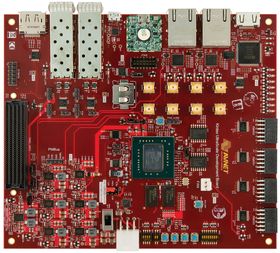
Kintex Ultrascale Ku040 Development Board
Aes Ku040 Db G By Avnet Engineering Services Evaluation Development Kits Avnet

Aes Ku040 Db G Avnet Development Kit Kintex Ultrascale Fpga High Performance Embedded Applications

Bck02 Fpga Xilinx Kintex Ultrascale Ku040 Like Aes Ku040 Db G Or Kcu105 For Sale Online Ebay

Kintex Fpga Ultrascale Data Center Board

Micromodule With Xilinx Kintex Ultrascale Ku040 1c 2 Gbyte Ddr4 4 X 5 Cm 4 X 5 Soms Trenz Electronic Products Trenz Electronic Gmbh Online Shop En

Fpga Hashdeploy

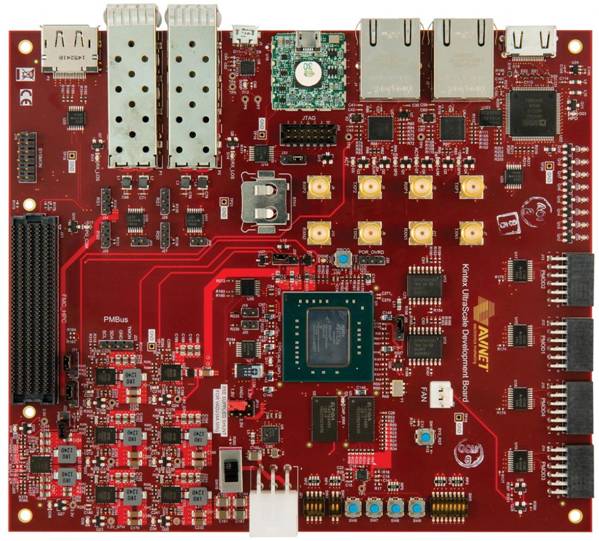
14 b kintex ultras cale development board coavnet0logo1.
Kintex ultrascale ku040 development board.

First Kintex Ultrascale Fpga Enters Full Productio Community Forums

Fpga Deployq Com

Xilinx Kintex Ultrascale Ddr4 Pcie 3 0 Fpga Board Similar With Ku040 Ebay
Xcell Daily Blog Archived Page 15 Community Forums

Xilinx Kintex Ultrascale Development Kit Aes Ku040 Db G Ebay
Xilinx Kintex Ultrascale Ku040 Fpga开发套件

Mikromodul Mit Xilinx Kintex Ultrascale Xcku040 1sfva784i 2 Gbyte Ddr4 Trenz Electronic Gmbh Online Shop En

Pmbus Power Architecture Introduction Youtube

Xilinx Kintex Xcku040 Fpga On Board For Sale Online Ebay

Design With Avnet Avnet

Te0841 Series Trenz Electronic Digikey

Kintex Ultrascale Board Ku040 Reference Design Bui Community Forums

Kintex Ultrascale De8040 Pcie Ddr4 Wan Wan Development Board Learning Board Aliexpress

Xcell Daily Blog Archived Page 26 Community Forums

Mellanox Connectx 4 Lx En Adds Local Application P Community Forums
Https Www Infineon Com Dgdl Infineon Xilinx Kintex Ultrascale Series Ati V01 00 En Pdf Fileid 5546d4625607bd1301565649617e0ca5

Xcell Daily Blog Archived Page 17 Community Forums

Ada Sdev Kit2 Fpga Board Xilinx Kintex Xqrku060 Space Grade Fpga Dev Kit

Xcell Daily Blog Archived Page 3 Community Forums
Https Si2 Epfl Ch Demichel Publications Archive 2017 Biocas 2017 Pdf

Kintex Fpga Ebay

Xcell Daily Blog Archived Page 22 Community Forums

Xilinx Ultrascale Programmable Logic Products Trenz Electronic Gmbh Online Shop En
Source : pinterest.com
